J. Semicond. >  Just Accepted

ARTICLES

Interface-engineered CVD graphene/WS2 heterostructures for transforming transient photodetection into optoelectronic synaptic plasticity

Yuning Li1, Xiaoqiu Tang1, Shengsheng Wei2, Yixin Zhang1, Yuyang Zhao1 and Tao Deng1,

+ Author Affiliations

 Corresponding author: Tao Deng, dengtao@bjtu.edu.cn

DOI: 10.1088/1674-4926/26090030CSTR: 32376.14.1674-4926.26090030

PDF

Turn off MathJax

Abstract: Artificial visual systems require both reversible optical perception and history-dependent information processing, which impose distinct requirements on photogenerated carrier dynamics. Here, we demonstrate that heterointerface engineering provides an effective strategy for regulating the temporal photoresponse of two-dimensional optoelectronic devices. Using CVD-grown WS2 as a common photosensitive material platform, we fabricated buried-gate WS2 photodetectors and graphene/WS2 van der Waals (vdW) heterostructure devices and systematically investigated their photoresponse characteristics. The WS2 device exhibits a positive and reversible photoconductive response under 365-660 nm illumination. In contrast, the introduction of graphene substantially modifies the photoresponse dynamics, giving rise to persistent photoconductivity and stimulus-history-dependent conductance modulation. The graphene/WS2 heterostructure exhibits continuously tunable short-term-plasticity- to long-term-plasticity-like behavior under variations in electrical bias, optical intensity, pulse number, and illumination duration, together with paired-pulse facilitation and learning-forgetting-relearning characteristics. Raman shifts and pronounced photoluminescence quenching after graphene integration further support substantial modification of the lattice and interfacial relaxation environment of WS2. These results demonstrate that heterointerface engineering can regulate photocarrier transport and relaxation across different time scales, providing a device-level strategy for bridging reversible photodetection and optoelectronic synaptic processing in artificial visual systems.

Keywords: interface engineering, heterostructures, optoelectronic synaptic, graphene/WS2


[1]
Liu J X, Li B, Liu C, et al. Devices, functions, and applications of artificial neuromorphic visual systems. Adv Sci, 2025, 12(46): e16379 doi: 10.1002/advs.202516379
[2]
Chen D K, Yu P Z, Li Y N, et al. Dedicated and reconfigurable artificial neurons and synapses based on two-dimensional materials for efficient neuromorphic application. Nano Micro Lett, 2026, 18(1): 310 doi: 10.1007/s40820-026-02139-2
[3]
Sun F Q, Wang Y Y, Zhao Z H, et al. Reconfigurable nonvolatile photodetectors for brain-inspired vision. ACS Nano, 2026, 20(30): 20937 doi: 10.1021/acsnano.6c08097
[4]
Hu Z Y, Zhang W C, Niu S, et al. Sensing–computing fusion in machine vision: A review on integrated systems and emerging devices. Adv Photonics Res, 2026, 7(4): e70207 doi: 10.1002/adpr.70207
[5]
Mennel L, Symonowicz J, Wachter S, et al. Ultrafast machine vision with 2D material neural network image sensors. Nature, 2020, 579(7797): 62 doi: 10.1038/s41586-020-2038-x
[6]
Zhu S R, Xie T, Lv Z Y, et al. Hierarchies in visual pathway: Functions and inspired artificial vision. Adv Mater, 2024, 36(6): 2301986 doi: 10.1002/adma.202301986
[7]
Zhou G D, Li J, Song Q L, et al. Full hardware implementation of neuromorphic visual system based on multimodal optoelectronic resistive memory arrays for versatile image processing. Nat Commun, 2023, 14: 8489 doi: 10.1038/s41467-023-43944-2
[8]
Huo P P, Zhang X H, Cui X Y, et al. Modulating persistent photoconductivity through barrier engineering for high-performance and multifunctional two-dimensional optoelectronic devices. Adv Sci, 2026, 13(27): e24279 doi: 10.1002/advs.202524279
[9]
Li M C, Gan Z X, Gui Q F, et al. Reconfigurable optoelectronic sensor with seven-order dynamic response time range for photodetection and neuromorphic visual perception within monolithic device. npj Nanophoton, 2026, 3: 33 doi: 10.1038/s44310-026-00123-7
[10]
Huo J L, Huo J P, Gao J, et al. Coupled ferroelectric-anisotropic optoelectronic synapse for polarization-sensitive neuromorphic vision. Nat Commun, 2026, 17(1): 1468 doi: 10.1038/s41467-025-68206-1
[11]
Ahn J, Yeon E, Hwang D K. Recent progress in 2D heterostructures for high-performance photodetectors and their applications. Adv Opt Mater, 2025, 13(13): 2403412 doi: 10.1002/adom.202403412
[12]
Xing R F, Zhang X L, Fan X S, et al. Coupling strategies of multi-physical fields in 2D materials-based photodetectors. Adv Mater, 2025, 37(16): 2501833 doi: 10.1002/adma.202501833
[13]
Han J Y, Fu Z Y, Wei J X, et al. 2D materials-based next-generation multidimensional photodetectors. Light Sci Appl, 2025, 14(1): 362 doi: 10.1038/s41377-025-01995-8
[14]
Sun X N, Hu Y F, Jiang C B, et al. Optoelectronic synapses based on two-dimensional transition metal dichalcogenides for neuromorphic applications. InfoScience, 2026, 3(1): e70005 doi: 10.1002/inc2.70005
[15]
Zeng L H, Tao L L, Tang C Y, et al. High-responsivity UV-vis photodetector based on transferable WS2 film deposited by magnetron sputtering. Sci Rep, 2016, 6: 20343 doi: 10.1038/srep20343
[16]
Ersu G, Doolan L, Pucher T, et al. Low-cost WS2 photodetector on water-soluble paper for transient electronics. Adv Funct Mater, 2025, 35(44): e09505 doi: 10.1002/adfm.202509505
[17]
Agunbiade G S, Zheng T, Zhao H. Stacking-polarity-controlled interlayer photocarrier dynamics in MoSe2/MoS2 heterostructures. Nano Lett, 2026, 26(23): 7564 doi: 10.1021/acs.nanolett.6c00898
[18]
Arora V, Nayak P K, Muthu D V S, et al. Twist-angle-dependent ultrafast transient dynamics of MoSe2/WSe2 van der Waals heterostructures beyond the exciton Mott transition. J Phys Chem C, 2025, 129(37): 16624 doi: 10.1021/acs.jpcc.5c03835
[19]
Li M J, Chu H L, Gao C F, et al. Bioinspired high-order in-sensor spatiotemporal enhancement in van der Waals optoelectronic neuromorphic electronics. Nat Commun, 2025, 16(1): 8801 doi: 10.1038/s41467-025-63873-6
[20]
Kim H C, Kim H, Lee J U, et al. Engineering optical and electronic properties of WS2 by varying the number of layers. ACS Nano, 2015, 9(7): 6854 doi: 10.1021/acsnano.5b01727
[21]
Wu H J, Lin Z C, Liu J X, et al. Ta2PdS6/MoS2 heterojunction phototransistor for high-performance photoelectric synapses and graphic identification. ACS Appl Mater Interfaces, 2025, 17(13): 20116 doi: 10.1021/acsami.5c01804
[22]
Zhao W, Ghorannevis Z, Chu L, et al. Evolution of electronic structure in atomically thin sheets of WS2 and WSe2. ACS Nano, 2013, 7(1): 791 doi: 10.1021/nn305275h
[23]
McCreary K M, Hanbicki A T, Singh S, et al. The effect of preparation conditions on Raman and photoluminescence of monolayer WS2. Sci Rep, 2016, 6: 35154 doi: 10.1038/srep35154
[24]
Gao Y, Liu Z, Sun D M, et al. Large-area synthesis of high-quality and uniform monolayer WS2 on reusable Au foils. Nat Commun, 2015, 6: 8569 doi: 10.1038/ncomms9569
[25]
Ferrari A C, Meyer J C, Scardaci V, et al. Raman spectrum of graphene and graphene layers. Phys Rev Lett, 2006, 97(18): 187401 doi: 10.1103/PhysRevLett.97.187401
[26]
He X, Li H, Zhu Z Y, et al. Strain engineering in monolayer WS2, MoS2, and the WS2/MoS2 heterostructure. Appl Phys Lett, 2016, 109(17): 173105 doi: 10.1063/1.4966218
[27]
Zhang R L, Gan L, Zhang D Y, et al. Disentangling light-induced charge transfer, heating, and strain effects in WS2/graphene heterostructures. Adv Materials Inter, 2023, 10(5): 2202013 doi: 10.1002/admi.202202013
[28]
Meng X, Du Y, Wu W, et al. Giant superlinear power dependence of photocurrent based on layered Ta2 NiS5 photodetector. Adv Sci, 2023, 10(20): e2300413 doi: 10.1002/advs.202300413
[29]
Lakhara A, Bhobe P A. Coexistence of ferromagnetism and enhanced photo-response in Fe-doped SnSe2 single crystals. Phys Chem Chem Phys, 2026, 28(2): 1148 doi: 10.1039/D5CP03461B
[30]
Kurtash V, Eliseyev I, Davydov V, et al. Twisted MoS2 bilayers as functional elements in memtransistors: Hysteresis, optical signatures, and photocurrent kinetics. Adv Elect Materials, 2026, 12(17): e00716 doi: 10.1002/aelm.202500716
[31]
Li X H, Lin Y H, Lin Z C, et al. Effect of stress modulation of Al2O3 and Si3N4 nanolayers on the photoelectric properties of ReS2 photodetectors based on sapphire substrates. J Alloys Compd, 2023, 969: 172347 doi: 10.1016/j.jallcom.2023.172347
[32]
Rani A, Verma A, Yadav B C. Substrate-engineered charge transport in Cu2S/WS2 nanohybrid self-powered photodetectors. Adv Mater Technol, 2026, 11(11): e02641 doi: 10.1002/admt.202502641
[33]
Siao M-D, Tsai M Y, Gandhi A C, et al. Two-dimensional phototransistors with van der Waals superstructure contacts for high-performance photosensing. ACS Appl Mater Interfaces, 2025, 17(4): 6521 doi: 10.1021/acsami.4c16883.s001
[34]
Knobloch T, Uzlu B, Illarionov Y Y, et al. Improving stability in two-dimensional transistors with amorphous gate oxides by Fermi-level tuning. Nat Electron, 2022, 5(6): 356 doi: 10.1038/s41928-022-00768-0
[35]
Fu S, du Fossé I, Jia X Y, et al. Long-lived charge separation following pump-wavelength–dependent ultrafast charge transfer in graphene/WS2 heterostructures. Sci Adv, 2021, 7(9): eabd9061 doi: 10.1126/sciadv.abd9061
[36]
Nandi S J, Ghosal S, Meyyappan M, et al. Defect-engineered 2D Bi2 Se3-based broadband optoelectronic synapses with ultralow energy consumption for neuromorphic computing. Mater Horiz, 2025, 12(12): 4274 doi: 10.1039/D4MH01625D
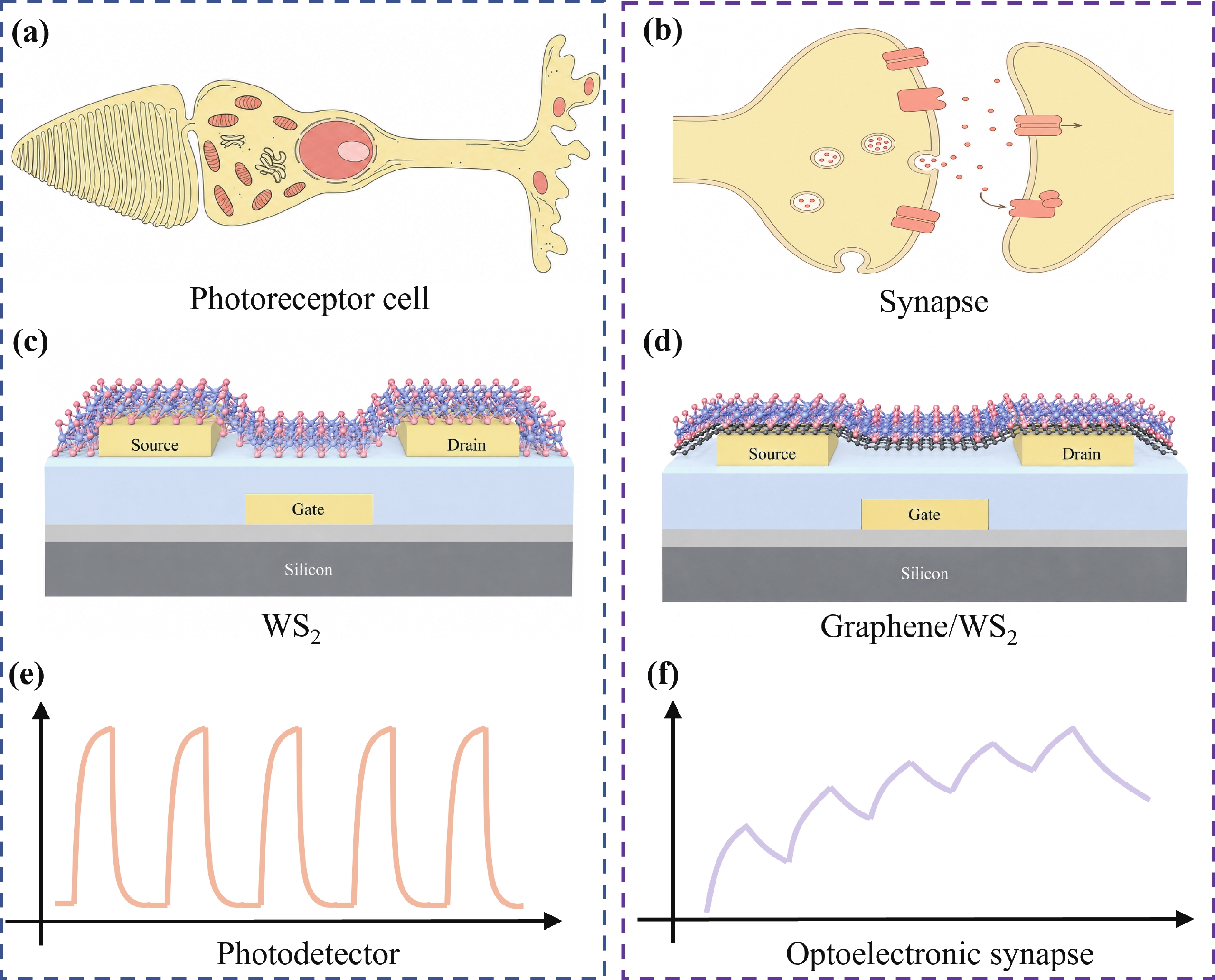
Fig. 1.  (Color online) Design and concept. (a) Photoreceptor cells and (b) synapse in biology. Schematic diagram of buried-gate (c) WS2 and (d) graphene/WS2 heterojunction devices for simulating photoreceptor cells and synapses, respectively. (e) Typical photoresponse curve of the WS2 photodetector. (f) Typical photoresponse curve of the graphene/WS2 optoelectronic synapse.

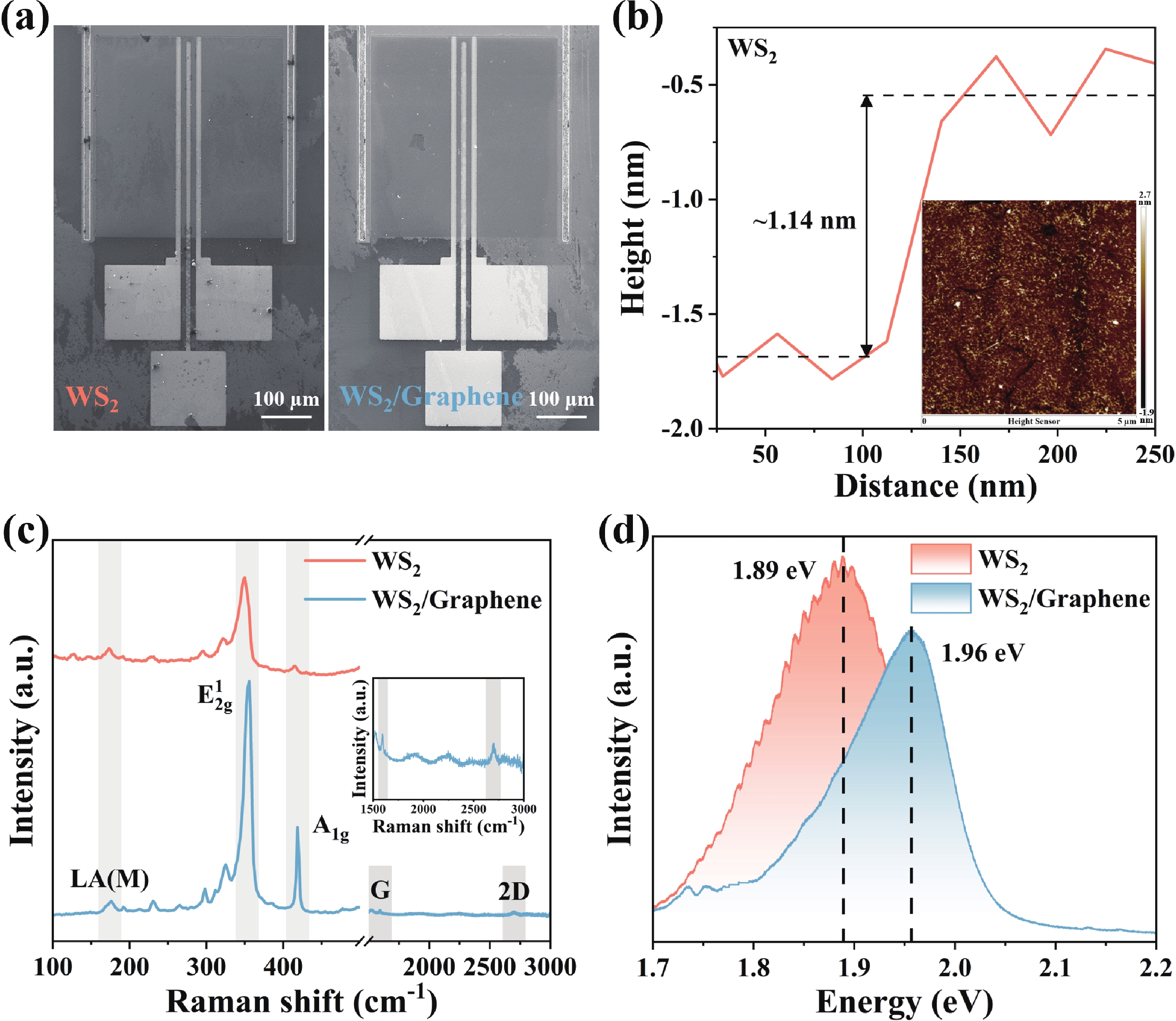
Fig. 2.  (Color online) Metrology and characterization. (a) Optical microimage of the buried-gate WS2 and graphene/WS2 heterojunction devices. (b) The height profile of the single-layer WS2. The inset shows the AFM topography image of the single-layer WS2. (c) Raman spectra of the conductive channel of the WS2 and graphene/WS2 heterojunction. (d) The PL spectrum of the WS2 and graphene/WS2 heterojunction.

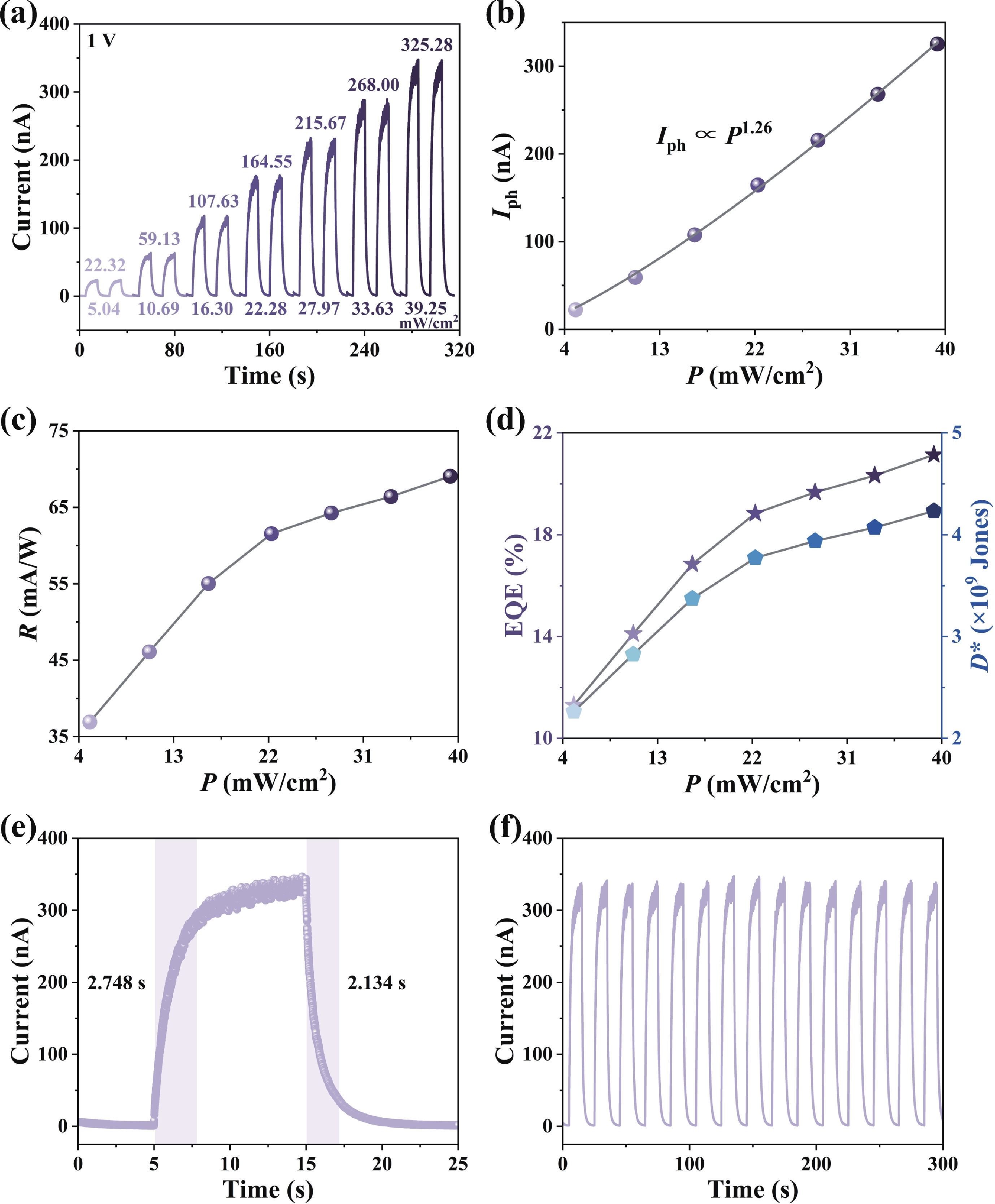
Fig. 3.  (Color online) Photoresponsive characteristics of the WS2 FETs under 405 nm illumination. (a) Measured current against the incident light power density at Vds=1 V and Vgs=0 V. (b) Photocurrent as a function of different power intensities. (c) Power-dependent photoresponsivity. (d) External quantum efficiency (EQE) and photodetection rate (D*). (e) A typical rising (τr) and falling times (τd) of the WS2 FETs photodetectors. (f) Time-dependent photocurrents of the WS2 FET.

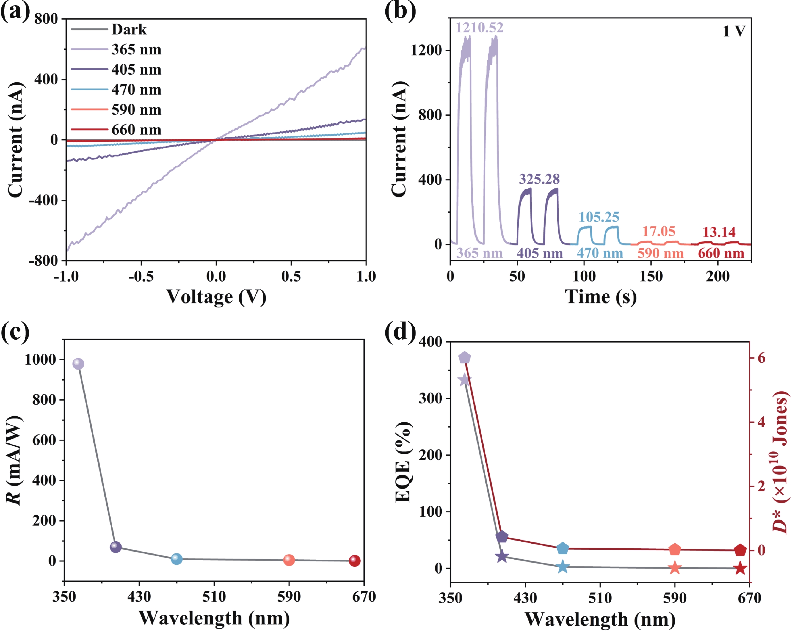
Fig. 4.  (Color online) Photocurrent and photoresponsivity of the WS2 FETs under different wavelengths. (a). The output characteristic curve under dark and different wavelengths (b) Measured current against the different wavelengths (365, 405, 470, 590, 660 nm) at Vds = 1 V and Vgs = 0 V. (c) Spectral dependence of the R. (d) EQE and D* as a function of excitation wavelength for the WS2 FETs photodetector.

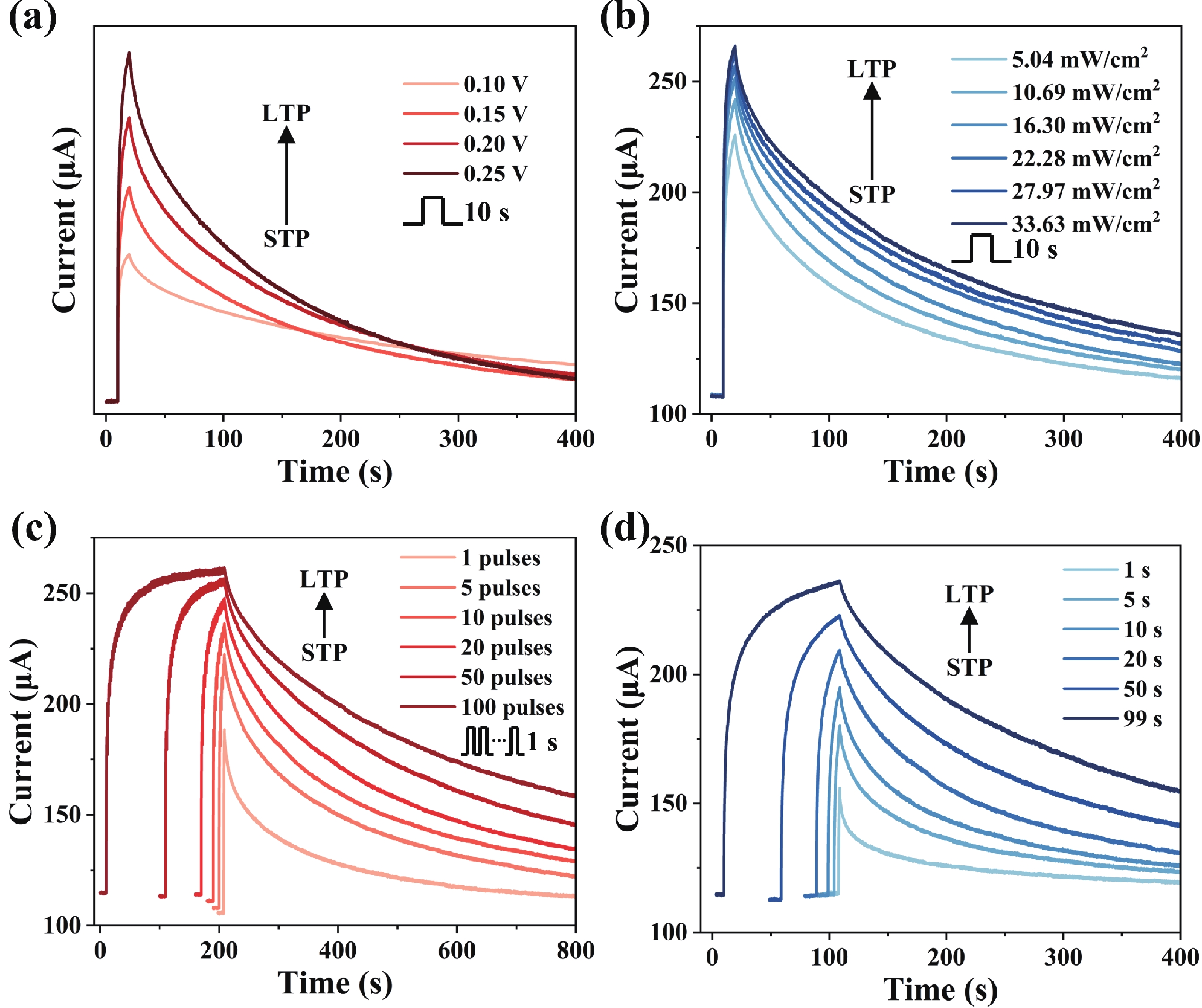
Fig. 5.  (Color online) Stimulus-dependent transition from short-term plasticity to long-term plasticity in the graphene/WS2 heterojunction. The STP-to-LTP transition induced by increasing (a) the source-drain voltage, (b) the incident light power density, (c) the number of the pulsed light stimuli, or (d) the illumination duration.

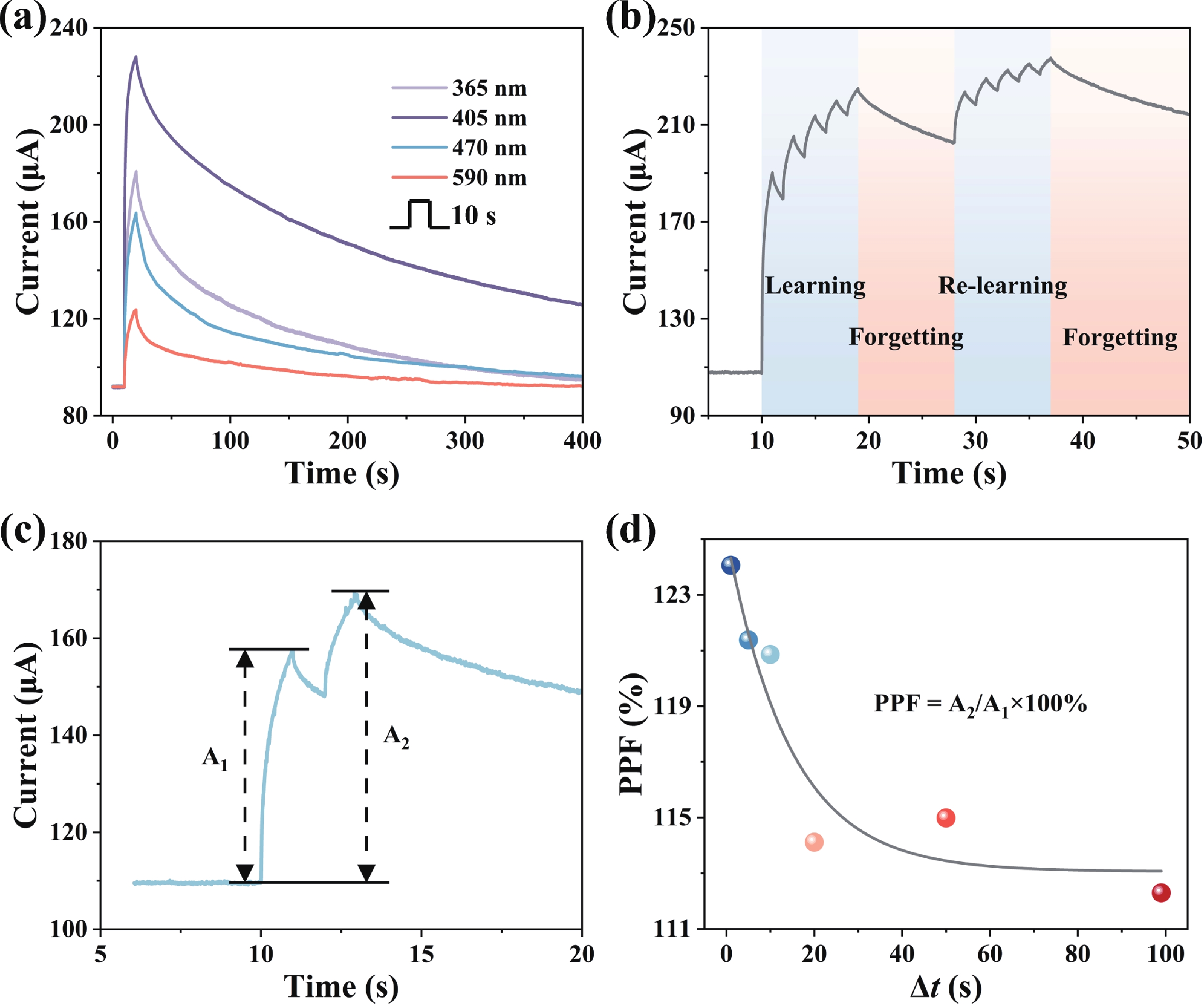
Fig. 6.  (Color online) (a) Typical photoresponsive characteristic under a light pulse pair. (b) PPF index of the the graphene/WS2 FETs for different Δt. (c) Ids with respect to time under different wavelength. (d) Classical memory curves simulation.

[1]
Liu J X, Li B, Liu C, et al. Devices, functions, and applications of artificial neuromorphic visual systems. Adv Sci, 2025, 12(46): e16379 doi: 10.1002/advs.202516379
[2]
Chen D K, Yu P Z, Li Y N, et al. Dedicated and reconfigurable artificial neurons and synapses based on two-dimensional materials for efficient neuromorphic application. Nano Micro Lett, 2026, 18(1): 310 doi: 10.1007/s40820-026-02139-2
[3]
Sun F Q, Wang Y Y, Zhao Z H, et al. Reconfigurable nonvolatile photodetectors for brain-inspired vision. ACS Nano, 2026, 20(30): 20937 doi: 10.1021/acsnano.6c08097
[4]
Hu Z Y, Zhang W C, Niu S, et al. Sensing–computing fusion in machine vision: A review on integrated systems and emerging devices. Adv Photonics Res, 2026, 7(4): e70207 doi: 10.1002/adpr.70207
[5]
Mennel L, Symonowicz J, Wachter S, et al. Ultrafast machine vision with 2D material neural network image sensors. Nature, 2020, 579(7797): 62 doi: 10.1038/s41586-020-2038-x
[6]
Zhu S R, Xie T, Lv Z Y, et al. Hierarchies in visual pathway: Functions and inspired artificial vision. Adv Mater, 2024, 36(6): 2301986 doi: 10.1002/adma.202301986
[7]
Zhou G D, Li J, Song Q L, et al. Full hardware implementation of neuromorphic visual system based on multimodal optoelectronic resistive memory arrays for versatile image processing. Nat Commun, 2023, 14: 8489 doi: 10.1038/s41467-023-43944-2
[8]
Huo P P, Zhang X H, Cui X Y, et al. Modulating persistent photoconductivity through barrier engineering for high-performance and multifunctional two-dimensional optoelectronic devices. Adv Sci, 2026, 13(27): e24279 doi: 10.1002/advs.202524279
[9]
Li M C, Gan Z X, Gui Q F, et al. Reconfigurable optoelectronic sensor with seven-order dynamic response time range for photodetection and neuromorphic visual perception within monolithic device. npj Nanophoton, 2026, 3: 33 doi: 10.1038/s44310-026-00123-7
[10]
Huo J L, Huo J P, Gao J, et al. Coupled ferroelectric-anisotropic optoelectronic synapse for polarization-sensitive neuromorphic vision. Nat Commun, 2026, 17(1): 1468 doi: 10.1038/s41467-025-68206-1
[11]
Ahn J, Yeon E, Hwang D K. Recent progress in 2D heterostructures for high-performance photodetectors and their applications. Adv Opt Mater, 2025, 13(13): 2403412 doi: 10.1002/adom.202403412
[12]
Xing R F, Zhang X L, Fan X S, et al. Coupling strategies of multi-physical fields in 2D materials-based photodetectors. Adv Mater, 2025, 37(16): 2501833 doi: 10.1002/adma.202501833
[13]
Han J Y, Fu Z Y, Wei J X, et al. 2D materials-based next-generation multidimensional photodetectors. Light Sci Appl, 2025, 14(1): 362 doi: 10.1038/s41377-025-01995-8
[14]
Sun X N, Hu Y F, Jiang C B, et al. Optoelectronic synapses based on two-dimensional transition metal dichalcogenides for neuromorphic applications. InfoScience, 2026, 3(1): e70005 doi: 10.1002/inc2.70005
[15]
Zeng L H, Tao L L, Tang C Y, et al. High-responsivity UV-vis photodetector based on transferable WS2 film deposited by magnetron sputtering. Sci Rep, 2016, 6: 20343 doi: 10.1038/srep20343
[16]
Ersu G, Doolan L, Pucher T, et al. Low-cost WS2 photodetector on water-soluble paper for transient electronics. Adv Funct Mater, 2025, 35(44): e09505 doi: 10.1002/adfm.202509505
[17]
Agunbiade G S, Zheng T, Zhao H. Stacking-polarity-controlled interlayer photocarrier dynamics in MoSe2/MoS2 heterostructures. Nano Lett, 2026, 26(23): 7564 doi: 10.1021/acs.nanolett.6c00898
[18]
Arora V, Nayak P K, Muthu D V S, et al. Twist-angle-dependent ultrafast transient dynamics of MoSe2/WSe2 van der Waals heterostructures beyond the exciton Mott transition. J Phys Chem C, 2025, 129(37): 16624 doi: 10.1021/acs.jpcc.5c03835
[19]
Li M J, Chu H L, Gao C F, et al. Bioinspired high-order in-sensor spatiotemporal enhancement in van der Waals optoelectronic neuromorphic electronics. Nat Commun, 2025, 16(1): 8801 doi: 10.1038/s41467-025-63873-6
[20]
Kim H C, Kim H, Lee J U, et al. Engineering optical and electronic properties of WS2 by varying the number of layers. ACS Nano, 2015, 9(7): 6854 doi: 10.1021/acsnano.5b01727
[21]
Wu H J, Lin Z C, Liu J X, et al. Ta2PdS6/MoS2 heterojunction phototransistor for high-performance photoelectric synapses and graphic identification. ACS Appl Mater Interfaces, 2025, 17(13): 20116 doi: 10.1021/acsami.5c01804
[22]
Zhao W, Ghorannevis Z, Chu L, et al. Evolution of electronic structure in atomically thin sheets of WS2 and WSe2. ACS Nano, 2013, 7(1): 791 doi: 10.1021/nn305275h
[23]
McCreary K M, Hanbicki A T, Singh S, et al. The effect of preparation conditions on Raman and photoluminescence of monolayer WS2. Sci Rep, 2016, 6: 35154 doi: 10.1038/srep35154
[24]
Gao Y, Liu Z, Sun D M, et al. Large-area synthesis of high-quality and uniform monolayer WS2 on reusable Au foils. Nat Commun, 2015, 6: 8569 doi: 10.1038/ncomms9569
[25]
Ferrari A C, Meyer J C, Scardaci V, et al. Raman spectrum of graphene and graphene layers. Phys Rev Lett, 2006, 97(18): 187401 doi: 10.1103/PhysRevLett.97.187401
[26]
He X, Li H, Zhu Z Y, et al. Strain engineering in monolayer WS2, MoS2, and the WS2/MoS2 heterostructure. Appl Phys Lett, 2016, 109(17): 173105 doi: 10.1063/1.4966218
[27]
Zhang R L, Gan L, Zhang D Y, et al. Disentangling light-induced charge transfer, heating, and strain effects in WS2/graphene heterostructures. Adv Materials Inter, 2023, 10(5): 2202013 doi: 10.1002/admi.202202013
[28]
Meng X, Du Y, Wu W, et al. Giant superlinear power dependence of photocurrent based on layered Ta2 NiS5 photodetector. Adv Sci, 2023, 10(20): e2300413 doi: 10.1002/advs.202300413
[29]
Lakhara A, Bhobe P A. Coexistence of ferromagnetism and enhanced photo-response in Fe-doped SnSe2 single crystals. Phys Chem Chem Phys, 2026, 28(2): 1148 doi: 10.1039/D5CP03461B
[30]
Kurtash V, Eliseyev I, Davydov V, et al. Twisted MoS2 bilayers as functional elements in memtransistors: Hysteresis, optical signatures, and photocurrent kinetics. Adv Elect Materials, 2026, 12(17): e00716 doi: 10.1002/aelm.202500716
[31]
Li X H, Lin Y H, Lin Z C, et al. Effect of stress modulation of Al2O3 and Si3N4 nanolayers on the photoelectric properties of ReS2 photodetectors based on sapphire substrates. J Alloys Compd, 2023, 969: 172347 doi: 10.1016/j.jallcom.2023.172347
[32]
Rani A, Verma A, Yadav B C. Substrate-engineered charge transport in Cu2S/WS2 nanohybrid self-powered photodetectors. Adv Mater Technol, 2026, 11(11): e02641 doi: 10.1002/admt.202502641
[33]
Siao M-D, Tsai M Y, Gandhi A C, et al. Two-dimensional phototransistors with van der Waals superstructure contacts for high-performance photosensing. ACS Appl Mater Interfaces, 2025, 17(4): 6521 doi: 10.1021/acsami.4c16883.s001
[34]
Knobloch T, Uzlu B, Illarionov Y Y, et al. Improving stability in two-dimensional transistors with amorphous gate oxides by Fermi-level tuning. Nat Electron, 2022, 5(6): 356 doi: 10.1038/s41928-022-00768-0
[35]
Fu S, du Fossé I, Jia X Y, et al. Long-lived charge separation following pump-wavelength–dependent ultrafast charge transfer in graphene/WS2 heterostructures. Sci Adv, 2021, 7(9): eabd9061 doi: 10.1126/sciadv.abd9061
[36]
Nandi S J, Ghosal S, Meyyappan M, et al. Defect-engineered 2D Bi2 Se3-based broadband optoelectronic synapses with ultralow energy consumption for neuromorphic computing. Mater Horiz, 2025, 12(12): 4274 doi: 10.1039/D4MH01625D

26090030-Supplementary Materials.pdf

  • Search

    Advanced Search >>

    GET CITATION

    shu

    Export: BibTex EndNote

    Article Metrics

    Article views: 4 Times PDF downloads: 2 Times Cited by: 0 Times

    History

    Received: 20 September 2026 Revised: 30 October 2026 Online: Accepted Manuscript: 17 November 2026

    Catalog

      Email This Article

      User name:
      Email:*请输入正确邮箱
      Code:*验证码错误
      Yuning Li, Xiaoqiu Tang, Shengsheng Wei, Yixin Zhang, Yuyang Zhao, Tao Deng. Interface-engineered CVD graphene/WS2 heterostructures for transforming transient photodetection into optoelectronic synaptic plasticity[J]. Journal of Semiconductors, 2026, In Press. doi: 10.1088/1674-4926/26090030 ****Y N Li, X Q Tang, S S Wei, Y X Zhang, Y Y Zhao, and T Deng, Interface-engineered CVD graphene/WS2 heterostructures for transforming transient photodetection into optoelectronic synaptic plasticity[J]. J. Semicond., 2026, accepted doi: 10.1088/1674-4926/26090030
      Citation:
      Yuning Li, Xiaoqiu Tang, Shengsheng Wei, Yixin Zhang, Yuyang Zhao, Tao Deng. Interface-engineered CVD graphene/WS2 heterostructures for transforming transient photodetection into optoelectronic synaptic plasticity[J]. Journal of Semiconductors, 2026, In Press. doi: 10.1088/1674-4926/26090030 ****
      Y N Li, X Q Tang, S S Wei, Y X Zhang, Y Y Zhao, and T Deng, Interface-engineered CVD graphene/WS2 heterostructures for transforming transient photodetection into optoelectronic synaptic plasticity[J]. J. Semicond., 2026, accepted doi: 10.1088/1674-4926/26090030

      Interface-engineered CVD graphene/WS2 heterostructures for transforming transient photodetection into optoelectronic synaptic plasticity

      DOI: 10.1088/1674-4926/26090030
      CSTR: 32376.14.1674-4926.26090030
      More Information
      • Yuning Li received the Ph.D. degree in electronics science and technology from Beijing Jiaotong University, Beijing, China, in 2025, where he is currently a postdoctoral researcher in Information and Communication Engineering at Beijing Jiaotong University. His research interests include MEMS sensors based on 2D materials
      • Xiaoqiu Tang got her Bachelor of Engineering degree in 2020 and Master of Engineering degree in 2023 from Dalian Jiaotong University. Now she is a doctoral student at Beijing Jiaotong University under the supervision of Prof. Tao Deng. Her research focuses on MEMS optoelectronic sensors
      • Tao Deng received the Ph.D. degree in electronic science and technology from Tsinghua University, Beijing, China, in 2015. Then, he joined Beijing Jiaotong University, Beijing, where he is currently a Full Professor of Fabrication and Characterization of MEMS Sensors. He has authored or coauthored more than 100 technical journal articles and conference presentations
      • Corresponding author: dengtao@bjtu.edu.cn
      • Received Date: 2026-09-20
      • Revised Date: 2026-10-30
      • Available Online: 2026-11-17

      Catalog

        /

        DownLoad:  Full-Size Img  PowerPoint
        Return
        Return